 |

21 Jul 2006
When it comes to cooling devices, common options include thermoelectric or Peltier methods but thin films of diamond are increasingly entering the equation. Matthew Peach speaks to Dwain Aidala, president and chief operating officer of sp3 Diamond Technologies, about the company's latest deposition reactor and its contribution to novel optical devices.
This article originally appeared in the July/August 2006 issue of Optics & Laser Europe magazine
While diamonds are prized by many for their appearance, the photonics market could soon be embracing the material as a thermal management solution thanks to properties such as a thermal conductivity four times that of copper.
One firm leading the way is sp3 Diamond Technologies of the US. The Santa Clara-based company provides diamond-based solutions for both research and production. Applications include electronics thermal management and diamond-on-silicon.
The company is working on diamond deposition techniques and the application of diamond coatings for a broad range of industrial uses. Examples include heat spreaders for laser diode mountings and fabricating silicon-diamond-silicon wafers for gallium nitride growth.
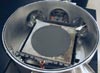
The latest development at sp3 is the Model 650 hot filament CVD diamond deposition reactor. The company claims that in its typical configuration, the 650 will be about half the price of other CVD deposition reactors that are based on microwave or high-pressure high-temperature designs.
sp3 says that the 650 offers precise control of the diamond film deposition and that the reactor can produce ultra-smooth nanocrystalline diamond coatings right through to rougher microcrystalline structures. It adds that film thickness can be controlled from 1000 Å to 100 µm with grain sizes from less than 10 nm to a size equal to the film thickness. Crucially, the company believes that the 650 will provide a route to higher output optical devices.
The 650 is a fourth-generation system that continues the established process automation and safety features of sp3's earlier reactors developed over the past 12 years. One notable addition is fully integrated process control, which allows both unattended operation and external monitoring.
MP: Why is diamond becoming such an important material for optical device developments?
DA: Diamond has many properties that lend it to a variety of applications, including its hardness, high stiffness and thermal conductivity, electrical conductivity or insulation for semiconductor applications, high bio-compatibility and extreme chemical resistance. In the MEMS area, its high Young's modulus of 1200 GPa is also of interest.
In optical applications, diamond's high thermal conductivity will enable higher emitter outputs by rapidly moving heat from the junction. This property will also contribute to higher device reliability. Another advantage of diamond is its ability to be an insulator or a conductor. It has a natural electrical resistivity of 1013 to 1016 ohm/cm. Furthermore, it can be made conductive by boron doping during the deposition process.
The company believes that the 650 will accelerate diamond's use in mainstream manufacturing by offering the most automated, scalable and flexible system available for CVD diamond deposition.
What are the implications for manufacturers and users of optical systems - can the release of the 650 lead to cheaper and better devices and components for optics-related applications?
Besides being used for the established cutting tool applications, the 650 is intended to be a platform for the development and early production of diamond-on-substrate work. It provides a device level thermal heat spreading layer for III-V material components such as GaAs and GaN lasers or LEDs. This is a route to higher output optical devices that are aimed at supplanting conventional illumination sources.
What are the key opportunities for the 650 diamond deposition system?
The radio frequency and power device markets are already moving down the road of integrating thermal management substrates into the active circuit. We expect that the optical markets will also begin exploring the integration of a thermal conduction layer into their designs as they continue to maximize lumens per watt. We are confident that the 650 will facilitate such investigations.
Is your deposition tool primarily for research and development or can it operate as a production volume tool?
The 650 is a continuation of sp3's involvement in the development and implementation of diamond applications. Since it can easily transition to a production platform, the 650 should reduce optical technology developers' common concerns about moving from device research and development towards production volumes.
We expect that the 650 will be purchased by companies aiming to differentiate themselves by using the special properties of diamond in areas such as MEMS, diamond-on- substrate and in the cutting of composite metal materials.
It is available in both a standard production configuration and a more flexible configuration for R&D applications. The R&D version adds an extra gas port for increased flexibility for development laboratories.
The device supports a uniform or mixed batch of irregular shaped substrates with proprietary fixturing while flat substrates are coated with the standard planar filament array fixturing package. An optional 3D filament array produces process uniformity without the complexity and reliability sacrifices of mechanisms inside the process chamber.
How is the current system an improvement on its predecessors?
Predecessors of the 650 have been used to grow thermal films on silicon wafers up to 300 mm in diameter, silicon-diamond-silicon wafers destined to be base wafers for GaN growth and nanocrystalline films designed specifically for MEMS wafers.
The new deposition system covers expanded applications such as diamond-on wafers in sizes up to 300 mm, wear coatings, substrates for thermal management, amorphous silicon deposition for solar cells and other products, electrodes for water treatment and electrochemistry and passivation layers for semiconductor chucks and cutting tools.
The 650 provides an integrated controller with a touch panel, streamlining the user interface. Additionally, it offers a network monitoring capability for increased data collection and analysis. This permits the transition from single development machine to multiple production machines in response to an important request from our current customers with multi-machine facilities.
What will the successful uptake of the 650 mean for sp3, in terms of business, growth and market reach?
We expect that substantial sales of the 650 will assist in our targeted penetration into the European market as well as expanding our presence in North America and Asia.
The device moves the development and manufacturing of CVD diamond fully into the 21st century. With its integrated graphical user interface controller and Ethernet conductivity, this is the most advanced deposition reactor for users who wish to take advantage of the many characteristics of diamond films.
 |  |  |  |  |  |  |
| © 2024 SPIE Europe |
|